Innolight's first near-package optics device enters early production on Tower's PH18M process
Tower Semiconductor and Innolight said on 3 November 2026 that Innolight's first near-package optics device entered early production on Tower's PH18M silicon photonics process in California, a step toward optical links for AI data centers.
 Rachel NwosuAI, models and technology
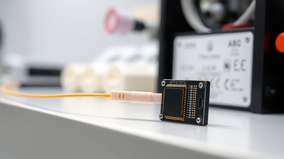
The device runs on Tower's PH18M process flow at its California factory, which uses a 200mm platform. Innolight has also completed tape-outs, or design submissions, for multiple NPO products on Tower's 300mm platform to support future product generations. The companies said the collaboration combines Innolight's optical interconnect designs with Tower's high-volume 200mm and 300mm manufacturing.
What near-package optics is
Near-package optics, or NPO, is an optical connectivity approach for AI infrastructure. The companies said NPO architectures are emerging as one of the preferred approaches for next-generation optical interconnects and are expected to drive additional demand beyond today's pluggable optical module market.
NPO designs typically require substantially higher optical channel counts than conventional pluggable modules, often integrating 16 or more channels on a single device, according to the companies. Tower said its silicon photonics platforms provide the process uniformity, yield performance and device range needed for those designs, and allow monolithic integration of photonic functions including wavelength division multiplexing and demultiplexing on one chip.
"Near-Package Optics is emerging as a key technology for next-generation AI and cloud infrastructure," Innolight CTO Oliver Sun said. "Our collaboration with Tower provides us with industry leading capabilities enabling us to accelerate the development of NPO solutions to meet the evolving needs of hyperscale and AI data center customers."
Why the milestone matters
The milestone covers Innolight's first NPO device, while the tape-outs on Tower's 300mm platform target later product generations. Tower is expanding that 300mm silicon photonics capacity in Japan, a planned $4 billion investment that includes about $1 billion in subsidies from Japan's Ministry of Economy, Trade and Industry and about $3 billion of Tower's own capital net of grants. Track One converts the Arai fab, formerly Fab 6, in Niigata Prefecture into a 300mm silicon photonics and advanced packaging site and expands Fab 7 in Uozu, Toyama Prefecture, with full production readiness targeted for the fourth quarter of 2027. Track Two, a new 300mm fab next to Fab 7, is subject to definitive agreements.
What happens next
The companies did not disclose production volumes for the early production device. Tower's Arai conversion is targeted for full production readiness in the fourth quarter of 2027, and the second Japan fab depends on agreements being signed and closed.
Sources
36- 01Tower Semiconductor and Innolight Advance High-Performance Near-Package Optics for AI InfrastructureEN
- 02Israeli foundry Tower Semiconductor to make Japan main hub for optical chipsEN
- 03Tower Semiconductor to establish large-scale optical chip hub as part of $4bn Japanese investment pledgeEN
- 04Tower Semiconductor revives shuttered Panasonic-era fab in $3 billion Japan photonics expansionEN
- 05Tower Semiconductor Japan Expansion Backed by $3 Billion Investment and METI SupportEN
- 06Tower Semiconductor Boosts 300mm Chip Production in JapanEN
- 07Mizuho bullish on Tower Semiconductor, points to AI optical growthEN
- 08Tower Semiconductor to make Japan its largest optical chip baseEN
- 092026 Global Semiconductor Industry Outlook - DeloitteEN
- 10Rapidus secures $1.7 billion from Japan’s government and private investors for 2nm chip production — company says it is in active discussions with more than 60 EN
- 11GlobalFoundries Wins $300M CHIPS Award to Scale Silicon Photonics for US AI Infrastructure - Tech TimesEN
- 12The US let Nvidia sell chips to an empty office in ChinaEN
- 13Human bodies produce 2 billion metric tons of CO2 a year just by staying aliveEN
- 14OpenAI lands an $11 billion funding round, but has to court dentists for more capitalEN
- 15OpenAI reportedly raises an additional $11 billion at a $1.25 trillion valuationEN
- 16TSMC is weighing a move into AI memory chips at Nvidia’s requestEN
- 17 Intel’s next-gen Nova Lake needs new motherboards — what we expect from Nova Point and Z990, Z970, and B960 chipsets EN
- 18Elon Musk's Tesla and SpaceX lose over $420 billion in combined market cap after midtermsEN
- 19Elon Musk’s nearly half a billion dollars in midterms spending was a flopEN
- 20Nabrawind’s Crane-Free Wind Towers Face a Supplier TestEN
- 21 Nintendo ROM chip supplier Macronix quits to focus on chips for AI data centers, reports indicate EN
- 22Cosmic at SEMICON Europa 2026: Advancing High-Complexity Semiconductor Test SolutionsEN
- 23Can Optical AI Cut Data Center Inference Power Use?EN
- 24China blocks SoftBank’s US$5.4 billion takeover of ABB’s robotics divisionEN
- 25Singapore Reveals Five-Year Energy Plan to Feed Data Center, Semicon ProgressEN
- 26$150 Billion More Paid by Americans for Gas This Year Than LastEN
- 27CesiumAstro Secures $730 Million in Janus Henderson-Led Series D at a Valuation Above $4.5 Billion; Unveils Synchronicity Satellite Constellation Following FullEN
- 28What Bangladeshi Prime Minister Tarique Rahman Brought Home From JapanEN
- 29AI Is Changing How Semiconductor Fabs Work — and Engineers Are Moving Faster Because of ItEN
- 30AI, fuelled by advanced chips, set to power semiconductor manufacturing: industry veteranEN
- 31Binance Reveals How Fake Job Interviews and AI Tool Abuse Led to $6.43 Billion TheftEN
- 32Marvell Proposes Acquiring Lumentum to Combine Optical Circuit Switching with AI Connectivity SiliconEN
- 33“People are getting spooked”: Tower CEO says AI demand remains intact - CTechEN
- 34China’s optical suppliers extend sell-off as fears of slower AI growth trump upbeat earningsEN
- 35Oracle Cloud to Offer Google TPUs and New AI ChipsEN
- 36Craft Prospect kicks off PERSEUS project to advance optical communications for spaceEN
All figures and quotations in this text come from the sources listed below.
Content prepared by the editorial team with AI assistance.
Rachel Nwosu
Comments
0- No comments yet — be the first.