European Commission approves €319m Austrian aid for Infineon's Villach GaN plant
The European Commission approved €319 million in Austrian state aid on 27 October for Infineon's €1.1 billion gallium nitride power semiconductor plant in Villach, a project the company calls the world's first high-volume 300mm GaN production.
 Rachel NwosuAI, models and technology
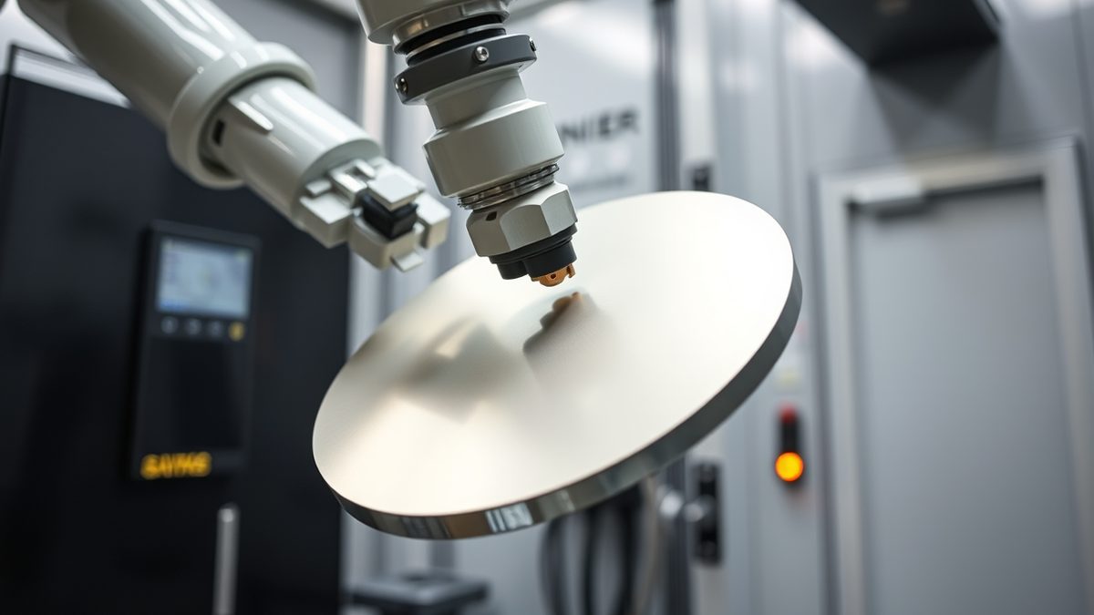
The Commission approved the aid on 27 October, the same day Infineon announced the investment at a Vienna news conference. Infineon will spend around €1.1 billion through 2034 to upgrade existing cleanrooms at Villach for high-volume gallium nitride power semiconductors on 300mm wafers. Production is scheduled to start by the end of 2027.
The aid covers just under 29 percent of the total, Austrian Economics Minister Wolfgang Hattmannsdorfer said. The Commission cleared it under the European Chips Act. Austria's Federal Ministry for Economic Affairs, Energy and Tourism still must issue a formal funding commitment, which Infineon says is expected within the stipulated time limits.
The Commission said the aid supports the expansion of the existing plant run by Infineon Technologies Austria AG. It said the project should generate benefits in related sectors through cross-border collaboration with universities and research institutions and improved access for start-ups and small and medium-sized enterprises.
Chancellor Christian Stocker called it one of the largest single investments in the history of Austria's high-tech industry. Infineon Austria employs around 5,800 people, including about 4,800 in Villach. Infineon Austria chief executive Sabine Herlitschka said the €1.1 billion investment will not create new jobs but will secure existing positions, according to dpa. She said the facility would help translate research into industrial production and support highly skilled employment.
The company is expanding Villach into a global center of excellence for power semiconductors. The project uses existing cleanroom space at Villach, which Infineon says makes the expansion cost-effective and efficient. It is far smaller than Infineon's new Dresden fab, which opened in the summer and cost around €5 billion, the largest single investment in the company's history.
Why 300mm GaN matters
GaN is a wide-bandgap material. Transistors made from it switch faster and lose less energy than silicon equivalents, so power supplies can be smaller and run cooler. Infineon is targeting AI data centers, energy infrastructure, electric mobility, robotics and consumer electronics.
The wafer size is the commercial argument. Infineon says a 300mm wafer yields about 2.3 times as many chips as a 200mm wafer. TechTimes reports that Infineon targets cost parity between GaN power switches and silicon MOSFETs at equivalent on-resistance below roughly 650 volts. If that holds, GaN could become the default in fast chargers, server power supplies and EV on-board chargers.
The manufacturing hurdle
GaN is not grown as a bulk crystal. It is deposited as a thin layer on a silicon wafer in a high-temperature process called MOCVD. GaN and silicon have a lattice mismatch of roughly 17 percent. As the wafer heats and cools, the two materials expand at different rates and stress builds with diameter.
Infineon's engineers describe the stress at 300mm as four elephants of about five tonnes each standing on a one Euro cent coin. Get it wrong and the wafer warps or the GaN film cracks. Infineon's Center of Competence for GaN Epitaxy in Villach developed buffer layers and process controls that manage the stress.
Infineon processed its first 300mm GaN wafers two years before the Villach announcement and announced pilot-line production in September 2024. The Villach project converts that pilot line into volume manufacturing. It uses existing 300mm silicon infrastructure rather than building a GaN fab from scratch.
Market and competition
Europe accounts for only around 10 percent of global chip production, Hattmannsdorfer said. He said every job in the chip industry can support six additional jobs across the broader economy. Yole Group expects the GaN power semiconductor market to reach about $3.5 billion by 2031, growing around 35 percent a year.
Competition is shifting. TSMC, the world's largest contract chipmaker, plans to exit the GaN foundry business by mid-2027, partly because of price pressure from Chinese rivals, TrendForce reported. China's Innoscience is the most prominent of those challengers. Navitas, STMicroelectronics and Texas Instruments are also working on GaN power chips. Infineon is betting that its early move to 300mm wafers will give it a cost advantage.
What happens next
Production is scheduled to start at the end of 2027, and Infineon says the ramp-up will be aligned with market demand rather than fixed to a volume target. The company says the plant will be the first worldwide to make GaN power electronics in volume on 300mm wafers, a claim the Commission repeats in its approval.
Infineon reports fourth-quarter and full-year 2026 results on 10 November, its next scheduled update on the business. The company lists the date as provisional in its financial calendar.
Sources
30- 01Infineon to Build Europe's First 300mm GaN Power Semiconductor FabEN
- 02Infineon Wins EU Funding for World's First 300mm GaN Factory: Silicon Cost Parity AheadEN
- 03Infineon to Invest 1.1 Billion Euros in Austrian GaN Chip PlantEN
- 04Infineon Invests 1.1 Billion Euros in European Semiconductors in Villach, AustriaEN
- 05Brussels Signs Off on EUR 319 Million for Infineon's Villach GaN PlantEN
- 06Infineon Puts €1.1 Billion Into a GaN Chip Factory in AustriaEN
- 07Infineon's Warstein Lab Opens as Intel Warning and AI Funding Fears Weigh on Chip SectorEN
- 08Infineon Charts EUR 1.1 Billion Villach Expansion While AI Power Deals Pile Up Ahead of November 10EN
- 09Infineon's EUR 1.1 Billion Villach Gamble Wins Brussels Blessing as GaN Era Takes ShapeEN
- 10Infineon invests 1.1 billion euros: The world's first 300-mm GaN volume production facility to be established in VillachEN
- 11 Nvidia can only fulfill 1% of China’s massive $70 billion GPU order for AI chips, report claims — supply constraints choke export-friendly RTX Pro 5500 deliverEN
- 12EU launches €525M platform to back European chip design start-upsEN
- 13Donnerstag: Millionen für europäische Chipdesigns, OpenAI mit GitHub-AlternativeEN
- 14Virtual power plants can help avoid overbuilt grid if AI boom goes bustEN
- 15Inside the chip talent war: Trade secrets and rising Chinese rivalsEN
- 16Chipfertigung: EU investiert Hunderte Millionen in Chipdesign-PlattformEN
- 17 Nintendo ROM chip supplier Macronix quits to focus on chips for AI data centers, reports indicate EN
- 18‘Every solar plant can be a data center’EN
- 19Binance attackers used fake job interviews to pull off $6.3 billion crypto heistEN
- 20A Michigan utility’s iffy plan to trap CO2 from its new gas plantsEN
- 21Accelerating Plug-And-Play Prototyping In Chiplet-Based DesignsEN
- 22Meta Raises €9 Billion as Euro Bond Debut Draws Record DemandEN
- 23Pure DC secures $1.9 billion financing for data center build-outEN
- 24Chiplets: Meta-Scale Chiplet Velocity Accelerating AI SoC Development to Match the Rapid Evolution of AI ModelEN
- 25Is There Room for Small-Scale OSATs in India’s Chip Packaging Boom?EN
- 26Binance co-CEO Richard Teng says hackers used fake job interviews, AI tool to steal $6.3 billion in crypto EN
- 27Meta seeks to raise up to $25 billion in debt sale as AI spending jumpsEN
- 28 AI chip smugglers exploit trade control loophole to bring banned HBM from South Korea into China EN
- 29$150 Billion More Paid by Americans for Gas This Year Than LastEN
- 30Kazakhstan Eyes Ambitious 2035 Goal for 2 Nuclear Power PlantsEN
All figures and quotations in this text come from the sources listed below.
Content prepared by the editorial team with AI assistance.
Rachel Nwosu
Comments
0- No comments yet — be the first.