IBM's Project SWIFT Ran a Layer in 5 Hours. Modern Fabs Take 19 to 36
Bill Harding's Project SWIFT averaged 5 hours per fabrication layer in the 1970s, IEEE Spectrum reports, while the fastest modern fabs take 19 hours and the industry average is 36.
 Grace OkonkwoAI, models and technology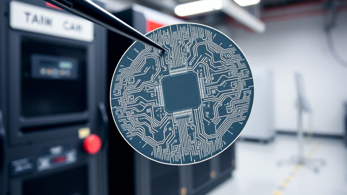
IBM's Project SWIFT averaged 5 hours to complete each layer of its fabrication process, IEEE Spectrum reported in December 2024. The fastest modern fabs take 19 hours per processing layer. The industry average is 36.
That gap is the hook of a long history piece by Jesse Aronstein, an engineer who worked on the programme. In 1970, Bill Harding, then manager of IBM's Manufacturing Research group in East Fishkill, New York, pitched a fully automated wafer-fabrication line that would turn out integrated circuits in less than one day. At the time, IEEE Spectrum writes, ICs such as random-access memory chips were typically produced in a monthlong stop-and-go march through dozens of manual work stations.
Harding was not a typical IBM manager. He grew up in Brooklyn, was wounded three times in combat in World War II while serving in George S. Patton's Third Army, and later earned bachelor's and master's degrees in mathematics and physics, according to the account. Aronstein first met him in 1962, when IBM was gearing up to produce the System/360, its first completely solid-state computer. The encounter was rough. Harding bellowed "What the hell good is that?" at Aronstein as he demonstrated how unpackaged semiconductor dice could be handled automatically in bulk for testing and sorting.
The comparison to today carries caveats that the article states plainly. Modern ICs are built with many more layers, on larger wafers, and the processing is more complex. IEEE Spectrum adds that those factors do not altogether close the gap. SWIFT's turnaround time, it says, has never been equaled.
What the rest of the supply chain is doing
The capacity question is not only about line speed. Governments and suppliers are spending on volume, materials and upstream inputs at the same time.
In Malaysia, second finance minister Amir Hamzah Azizan told CNBC at the IMF spring meetings in Washington in April 2024 that the country is unfazed by competition from China or the US as it pushes into higher-end semiconductor manufacturing. "The semiconductor space is now in the upcycle, and Malaysia will be a beneficiary of that," he said. Malaysia holds 13% of the global market for chip packaging, assembly and testing services, according to a Malaysian Investment Development Authority report cited by CNBC in February.
"We're seeing a lot of end users now diversifying their supply chain. Our focus, actually, is to provide a very vibrant, strong supply chain connectivity, and make sure that we ride on that."
Amir Hamzah also said Malaysia would not go "head on to the tail end of the high-end competition, where maybe the US is bringing all the parts."
India is taking a different route. TechCrunch reported on 15 July 2026 that New Delhi unveiled a ₹625 billion (about $6.5 billion) Mobile Phone Manufacturing Scheme, running five years, with incentives of 2.25% to 5% on eligible sales and an extra 1.5% for sourcing key components and sub-assemblies locally. The same announcement committed a further ₹1.28 trillion (around $13.3 billion) to domestic semiconductor manufacturing, expanding a $10 billion chip incentive programme launched in 2021. India accounted for 18% of global smartphone production in 2025, against China's 63%, according to Counterpoint Research.
On the component side, Texas Instruments said on 24 October 2024 that it had started producing gallium nitride power semiconductors at its factory in Aizu, Japan, quadrupling internal GaN capacity across its US and Japanese sites. Mohammad Yunus, TI's senior vice president of technology and manufacturing, said the company aims to grow internal manufacturing to more than 95% by 2030. TI also said it had piloted GaN processes on 300mm wafers.
The input nobody can substitute quickly
Then there is quartz. Spruce Pine, North Carolina, is home to high-purity quartz mines operated by Sibelco North America and The Quartz Corp. Tom's Hardware reported on 1 October 2024 that Hurricane Helene brought over two feet of rain to the town, cutting off roads and leaving residents without power, and that Sibelco had confirmed a suspension of operations. The Quartz Corp told The Verge it was too early to say whether its production facility was affected.
Construction Physics examined the claim that all semiconductor manufacturing depends on Spruce Pine. Its November 2024 assessment: quartz crucibles are indeed necessary for most semiconductor manufacturing, and Spruce Pine is where most of the quartz comes from, but the town is not quite an irreplaceable linchpin. Cutting off supply probably would not choke off semiconductors completely. It would mean yields going down and costs going up. New sources of quartz are being developed and new crucible materials investigated.
The details in that piece are worth keeping. High-purity quartz costs on the order of $10,000 a ton, crucibles cost several thousand dollars apiece, and a crucible is limited to around 400 hours of operation. A Czochralski furnace consumes 20 to 25 crucibles a year. One paper cited by Construction Physics estimated that 30% of the manufacturing cost of monocrystalline silicon ingots came from the crucibles.
Put the numbers together and the picture is less dramatic than the headlines that followed Helene. Spruce Pine is estimated to produce 180,000 to 200,000 tons of high-purity quartz per year, up from roughly 30,000 tons of high-purity output in 2015. That is a lot of material for an industry this size, and very little next to a coal mine.
The harder question is the one SWIFT raises. Automation of the kind Harding built has spread across the industry, IEEE Spectrum notes, and many of his line's innovations are now commonplace. The turnaround time is the part that did not travel.
Sources
6- 01IBM invented semiconductor manufacturing automationEN
- 02Malaysia pushes into higher-end semiconductor manufacturingEN
- 03Hurricane devastates quartz mines critical for semiconductor manufacturingEN
- 04India to allocate $20B to semiconductor and smartphone manufacturingEN
- 05TI expands internal manufacturing for gallium nitride (GaN) semiconductorsEN
- 06Does All Semiconductor Manufacturing Depend on Spruce Pine Quartz?EN
All figures and quotations in this text come from the sources listed below.
Content prepared by the editorial team with AI assistance.
Grace Okonkwo
Comments
0- No comments yet — be the first.