What is an AI accelerator? Inside the chips that run datacenter inference
AI accelerators are the specialised chips that sit next to regular CPUs in datacenter racks and do the matrix maths behind chatbots and image generators. How they are built, and who can build them, is more interesting than the acronyms suggest.
 Rachel NwosuAI, models and technology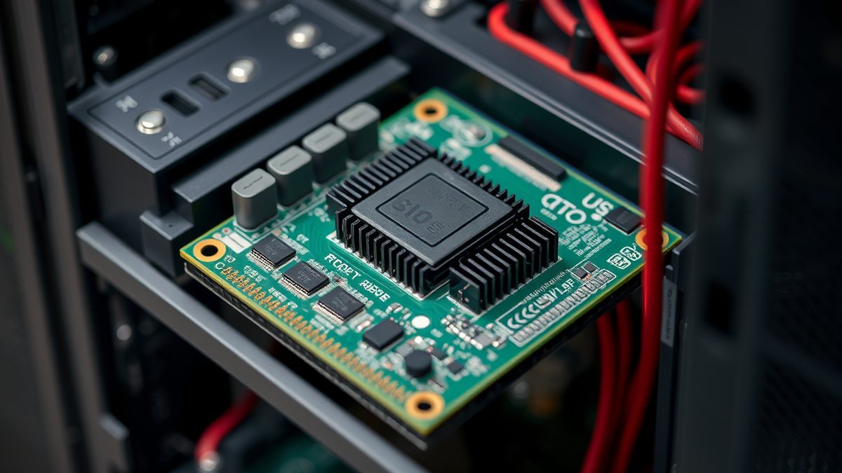
Every large language model you have used was almost certainly served by a chip that is not a CPU. It is an accelerator: silicon built to do one kind of arithmetic, matrix multiplication, very fast. The rest of the machine exists to keep it fed. That division of labour explains most of the recent drama in the datacenter market. It also explains why companies that once sold CPU cores, memory or packaging now argue about teraFLOPS, memory bandwidth and how many banks fit on a DRAM die.
The basic block, and why SiFive is now selling one
SiFive spent years licensing RISC-V CPU cores that other companies attached to their own AI engines. According to The Register, at least some of Google's tensor processing units use SiFive's X280 cores to manage the machine-learning accelerators and keep their matrix multiplication units fed. John Ronco, SVP and GM of SiFive UK, told the publication that SiFive's designs also underpin the CPU cores in Tenstorrent's Blackhole accelerator.
In September 2024 the company changed position. It announced the Intelligence XM series, a licensable AI accelerator cluster rather than just the CPU part. The base cluster contains four Intelligence X RISC-V CPU cores connected to an in-house matrix math engine. Each cluster supports up to 1TB/sec of memory bandwidth. The Register's write-up says it should deliver up to 16 TOPS of INT8 or 8 teraFLOPS of BF16 per gigahertz.
"For some customers, it's still going to be right for them to do their own hardware," Ronco said. "But, for some customers, they wanted more of a one-stop shop from SiFive."
That per-gigahertz figure looks odd at first. It is a building block, not a chip. The Register notes that SiFive expects most chips based on the design to run at around 1GHz, and that Ronco expects four to eight clusters per chip. At eight clusters and 1GHz, that is up to 64 teraFLOPS of BF16. The product slide deck suggests 512 clusters is possible. The Register calculates that would reach roughly four petaFLOPS of BF16 matrix compute, above the 2.5 petaFLOPS Nvidia quotes for its top-specced Blackwell GPUs. Those numbers are theoretical. Real performance depends on the clock, the power and cooling budget, the process node and what else shares the die. SiFive also says it will publish an open source reference implementation of its SiFive Kernel Library to lower the barrier to RISC-V adoption.
Inference is a memory problem before it is a maths problem
Accelerator vendors spend less time talking about raw compute now and more about memory, because that is where inference actually slows down. d-Matrix used its Hot Chips 2026 presentation to lay out the arithmetic: model weights keep growing, and the KV cache scales with context length multiplied by batch size. ServeTheHome reports d-Matrix's example of 64 users at 1M context producing roughly 935GB of KV cache. Capacity and bandwidth both become problems, and both keep growing.
SRAM meets the bandwidth target but holds almost nothing: about 4GB for a Corsair card pair at roughly 300 TB/s and 1ns latency, according to ServeTheHome. A 6T SRAM cell is about 10 times larger than a DRAM cell. HBM solves capacity but hits a practical bandwidth ceiling around 20 TB/s for HBM4 packages such as Nvidia's Vera Rubin and AMD's Instinct MI455. HBM bandwidth also carries a power cost: at 2.4 pJ/bit, pushing 100 TB/s through HBM consumes about 1.92 kW before fabric traffic.
d-Matrix's answer is to stack compute directly on DRAM dies. The company says a 1-Hi logic-on-top stack at no more than 0.5 W/mm2 can be liquid cooled and keep DRAM under 100C. Vertical 3D IO lands around 0.3 to 0.4 pJ, roughly 10 times lower than HBM. Its Raptor implementation puts a TSMC N4 logic die on a 3D DRAM die using 36um face-to-face stacking. A 72-card scale-up is sized to host a frontier model such as Kimi K3 at 1M context, with 32GB per card using 4-bit weights and an 8-bit KV cache. The engineering detail matters because it shows how much of accelerator design is now about data movement rather than multiply-accumulate units. d-Matrix's die has 840 banks, 768 after spares, across 256 channels, which works out to 3 banks per channel. Delivering a 128B flit from 32B banks therefore needs two accesses and fetches 192B, wasting about 33 percent of bandwidth near 33 TB/s. Stream blocking reclaims it by sharing one partial 32B access across three flits.
Packaging, not just silicon
There is a second constraint that has nothing to do with chip design. Tom's Hardware reported in March 2026 that Nittobo, a Japanese company, controls roughly 90 percent of the global supply of T-glass, a low-CTE glass-fibre cloth used in the organic core of IC substrates. Every advanced AI chip package contains it. Demand is outstripping supply.
The numbers are blunt. Nittobo is tripling capacity at its Fukushima plant, but the new supply will not reach the market until mid-2027. Prices have risen 20 to 30 percent, and lead times for downstream materials such as copper-clad laminates have stretched from a normal 8 to 10 weeks to beyond 20. Tom's Hardware cites data from Nvidia showing interposer sizes have grown from 814mm2 for Hopper to 1,700mm2 for Blackwell, a 109 percent increase, with Rubin and Feynman scaling further.
"With T-glass supply even more constrained now, suppliers are no longer providing lead times," said Bill Ho, analyst at Yuanta.
Nittobo is doubling raw yarn capacity at its Taiwan plant and has struck a collaboration deal with Nanya Plastics to outsource some weaving. According to Tom's Hardware, roughly 20 percent of Nittobo's glass cloth is expected to be woven by Nanya by 2027. Bank of America estimates Nittobo's electronic materials segment will nearly double sales from 40.9 billion yen in 2025 to 87.7 billion yen by March 2028, with operating margins approaching 48 percent.
Who is actually shipping
While all this is being argued over, some startups are putting silicon in front of audiences. According to ServeTheHome, Rebellions showed its REBEL-Quad accelerator running at Hot Chips 2025: four compute ASICs, four HBM3E sites for 144GB of memory, built on Samsung SF4X and CoWoS-S, with UCIe-A as the chiplet interconnect and a dual PCIe Gen5 x16 interface. The company ran a live Llama 3.3 70B demo on a development board at 35.5 msec average per output token. ServeTheHome noted that many accelerator companies never get as far as a public running demo.
On the client side, Draw Things reported that Metal FlashAttention v2.5 with Neural Accelerators delivers up to 4.6 times better performance on Apple's M5 than on M4, with raw improvements of 3.6 to 5.5 times and end-to-end gains of 3.3 to 4.6 times on an M5 iPad. The software is a preview: BF16 support was initially disabled because of unsolved bugs, and shaders take longer to specialise. The measurements were taken with an ice pad under the iPad for maximum cooling, which says as much about thermal headroom as about the chip.
None of this settles which architecture wins. It does show that the datacenter accelerator is no longer a single product category. It is a stack of CPU cores, matrix engines, memory technology, packaging materials and software libraries, each with its own bottleneck and its own lead times.
Sources
5- 01SiFive shifts from RISC-V cores for AI chips to designing its own acceleratorEN
- 02Shortages of crucial chip packaging material threatens AI accelerator supplyEN
- 03d-Matrix Raptor 3D-DRAM Accelerator for Generative Inference at Hot Chips 2026EN
- 04Rebellions REBEL-Quad UCIe and 144GB HBM3E Accelerator at Hot Chips 2025EN
- 05Metal FlashAttention v2.5 with Neural Accelerators on the Apple M5 ChipEN
All figures and quotations in this text come from the sources listed below.
Content prepared by the editorial team with AI assistance.
Rachel Nwosu
Comments
0- No comments yet — be the first.