India's chip packaging push: small OSATs and Odisha's $4 billion pipeline
India's outsourced semiconductor assembly and test sector is opening room for smaller, specialised packaging plants, EE Times reported on 3 November. Sahasra Semiconductors' plant in Bhiwadi, Rajasthan, was built on more than ₹1.5 billion, about $15.8 million.
 Dr. Amara PatelEconomy, business and world
Small packaging plants get a policy opening
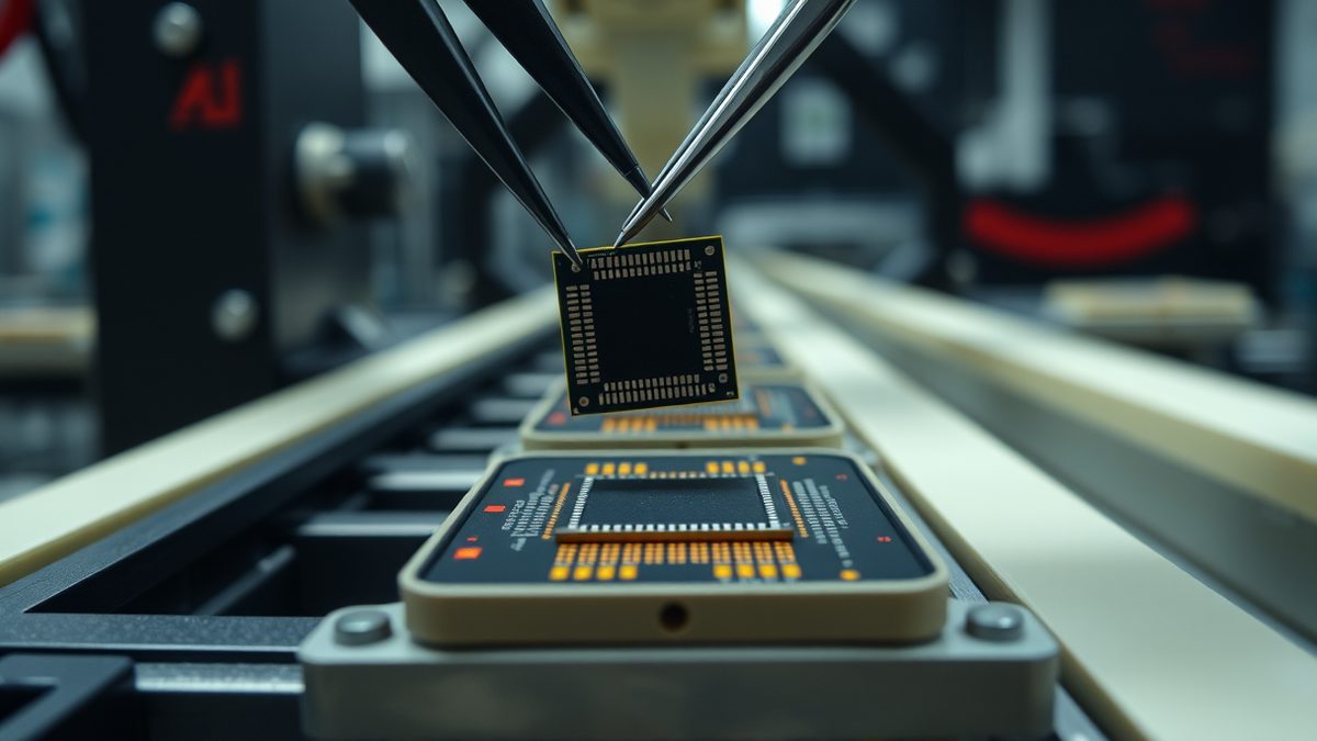
India's outsourced semiconductor assembly and test industry is making space for smaller, specialised packaging plants, EE Times reported on 3 November.
The test for buyers and investors is simple. Can India build packaging capacity that wins long-term customers, rather than only announce fabs? Odisha's five projects would spread chip work beyond existing clusters. The state has not given start dates or named customers for them. A new packaging plant needs an anchor customer committed for three to five years, according to consultant Nitin Dodia.
Sahasra Semiconductors runs one such plant in Bhiwadi, Rajasthan. It was built on an investment of more than ₹1.5 billion, about $15.8 million, according to a May 2026 government announcement. The facility covers 5,295 square metres, or 57,000 square feet, and has a stated annual packaging capacity of 60 million units. It packages memory chips for microSD cards and flash storage, LED driver ICs, eSIMs and RFID products. The plant was set up under the Ministry of Electronics and Information Technology's SPECS scheme. The government described Sahasra as India's first small and medium enterprise to begin commercial production of semiconductor chips.
Dodia is founder-director of Smart Fab Systems. He estimated a mature packaging facility could be set up for ₹1.5 billion to ₹2 billion, about $15.8 million to $21 million.
Dodia said production volume drives capital expenditure. Simple wire bonding or leadframe-based packaging is less capital intensive, he said. A company such as Micron processes millions of chips a month and needs equipment built for those volumes. Specialist plants on mature technologies can start far lower, he said.
RRP Electronics runs an OSAT facility in Mahape, Navi Mumbai. It serves automotive, industrial and telecom customers.
Odisha puts five chip projects on the table
Odisha is planning five semiconductor projects involving more than $4 billion.
State officials set out the pipeline at TiECon Bhubaneswar 2026 on Friday, 30 October. The projects include India's first compound semiconductor fabrication unit and its first advanced 3D chip packaging facility. Vishal Kumar Dev is Additional Chief Secretary of the state's Electronics and IT Department. He said two of the 12 projects approved under the India Semiconductor Mission are coming up in Odisha. He said groundwork began within six to eight months of approval. Dev also cited collaborations with Intel and 3D Glass Solutions on advanced packaging.
The projects span fabrication, advanced packaging and artificial intelligence infrastructure. Officials position them as a shift from Odisha's mining and metals base toward technology-driven industries.
The state's pitch goes beyond fabs. Odisha has formulated an AI policy and announced an Odisha AI Mission. Officials are also chasing AI data centres, research infrastructure and global capability centres. Electronics and IT Minister Mukesh Mahaling cited land availability, surplus electricity and natural resources as advantages.
No start date has been given for the five projects.
The scale gap between small and large OSATs
Sahasra's annual capacity is 60 million units. That is about 164,000 units a day. The large plants are built for a different order of volume:
- Tata Electronics' facility in Assam, worth ₹270 billion (about $3.25 billion), has an approved capacity of 48 million units a day.
- CG Power's plant in Sanand, Gujarat, worth ₹76 billion (about $910 million), is planned for 15 million units a day.
- Kaynes Technology's facility, also in Sanand, worth ₹33.07 billion (about $395 million), is designed for more than 6.33 million units a day.
Tata's approved daily capacity exceeds Sahasra's annual capacity many times over.
Capability and customer tests remain
Dodia made a broader point.
"The bigger point, however, is that success is not just about money," he said.
He said a new OSAT should secure at least one customer committed to buying its products over three to five years. Capacity utilisation, experienced personnel and product qualification matter as much as the equipment list, he added. An investor could spend ₹1 billion to ₹2 billion, about $11 million to $21 million, on tools. Idle equipment will not deliver returns without customers.
Sahasra and RRP Electronics have an advantage, Dodia said. They entered earlier and already have customers buying their products.
India needs capabilities beyond chip design, the Semi-Conductor Laboratory's director general said. A report on 31 October carried the remark. Zuvay Technologies aims by 2030 to become an engineering and equipment partner for India's GW-scale solar manufacturing while building capabilities in semiconductor manufacturing. Its work spans wafer and cell-line configuration, automation, cleanroom and HVAC, and gas abatement systems for TOPCon and PERC lines. The company says its parametric engineering tools, which derive facility utilities from cell-line capacity, are transferable to semiconductor front-end infrastructure. The company frames it as a matter of tolerances. It is not new physics, it says.
Sources
28- 01Is There Room for Small-Scale OSATs in India's Chip Packaging Boom?EN
- 02India needs capabilities beyond chip design, says Semi-Conductor Laboratory DG: ReportEN
- 03ZUVAY TECHNOLOGIES: Engineering India's Path from Solar Manufacturing to Semiconductor InfrastructureEN
- 04Copeland Expands Scroll Compressor Manufacturing in India - Construction WorldEN
- 05Odisha's $4 Billion Semiconductor Push: 5 Projects Could Put State on India's Chip Manufacturing MapEN
- 06 Apple faces unprecedented memory cost increases as RAM prices continue to surge, manufacturing bill climbs by $33 billion EN
- 07Waaree doubles Texas solar module manufacturing capacity to 3.2 GWEN
- 08India’s Critical Minerals Industrial Policy Balances Domestic Ambitions and Transnational Challenges - CGEPEN
- 09Yingfa Ruineng establishes 7.5 GW PV manufacturing plant in IndonesiaEN
- 10Rayzon Solar to start production at 5.1 GW TOPCon cell facility in December, plans ingot-wafer manufacturing by 2028 - pv magazine GlobalEN
- 11Google takes Dreambeans to India in bid to bring AI-generated personal stories to the massesEN
- 12U.S. Manufacturing Activity Gains Momentum in OctoberEN
- 13Foxconn details quantum ambitions, wants to become world’s “largest quantum computer manufacturer”EN
- 14IEA: India Can Help Diversify Global Solar PV Supply ChainsEN
- 15PVLB.I 2026: TaiyangNews Briefing Focuses On India’s Solar GrowthEN
- 16India’s new-age manufacturers to benefit from $3 trillion global AI investment cycle: Avendus CapitalEN
- 17Marvell to buy Lumentum in $115 billion deal in AI data-centre bet - ET ManufacturingEN
- 18Electronic equipment maker Keysight taps insider Jason Kary as finance chief - ET ManufacturingEN
- 19‘The Indian Question’: The Rise of Anti-Indian Hate in AmericaEN
- 20Inside Automotive DMS & OMS: Technology, Challenges & Power Solutions EN
- 21In Memory of Fukuda Diplomacy: Peace, History, and Japan’s Foreign PolicyEN
- 22 India launches next-gen navigation satellite to orbit (video) EN
- 23How Beta Technologies Is Clearing the Runway for Electric FlightEN
- 24India’s China+1 Dilemma: It May Need China to Depend Less on ChinaEN
- 25American Tech Needs A Trusted Second Home — India Can Earn ItEN
- 26India, Germany to deepen investment ties, strengthen cooperation in emerging tech, manufacturingEN
- 27Kumaraswamy urges auto industry to invest in EV technologies, batteries and hydrogen - ET AutoEN
- 28Amid India–China Border Tensions, Mega Hydel Project in Arunachal Pradesh Faces Local HeatEN
All figures and quotations in this text come from the sources listed below.
Content prepared by the editorial team with AI assistance.
Dr. Amara Patel
Comments
0- No comments yet — be the first.