Chip packaging is the new bottleneck: 17.5 GW of AI datacenter power, and that is the ceiling
Advanced packaging capacity in place today can support accelerators drawing roughly 13 GW of gross power, which works out to about 17.5 GW of total datacenter power once CPUs, memory and cooling are counted, according to numbers The Register reported on 30 September from investment bank Jefferies and analytics firm SynMax.
 Grace OkonkwoAI, models and technology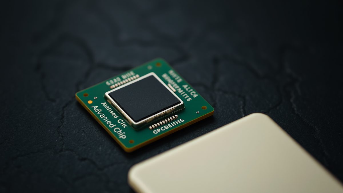
That is the number that matters. Not the announced pipeline, not the 80 GW that some 2028 demand models imply. The packaging ceiling.
Jefferies shared the report with The Register, which published it on 30 September. SynMax, which tracks weekly satellite imagery of land clearing, first structures and construction progress, estimates US deployments will rise from roughly 11 GW of gross capacity in 2025 to 16-18 GW in 2026, above its earlier forecast of 14-16 GW. It puts the practical upper limit for 2027 in the low 20s of gigawatts. Two more packaging projects expected online in 2027 could add another 6 GW, but only if capacity expands faster than forecast. The gap between land and silicon is now visible from orbit. Land clearing for new projects has plateaued, The Register reported, leaving visible activity well short of the pace required to deliver the more than 80 GW implied by announced pipelines. A previous Jefferies report found only half the US capacity scheduled for 2026 was under construction, and work had yet to begin on as much as 80 percent of the 2028 pipeline.
Why packaging, not wafers
Fabricating accelerator dies is only half the job. They must then be packaged with components such as high-bandwidth memory before OEMs can install them in servers.
Advanced packaging combines multiple dies and memory using high-density connections, an approach used in many advanced CPUs and AI accelerators. Even chips manufactured on US soil may need to be sent overseas, typically to Taiwan, for packaging, creating a choke point between semiconductor production and operational datacenter capacity.
At A*STAR's Innovate Together 2026 in Singapore, engineers from KLA, ASM, ASMPT and the National University of Singapore described the squeeze in process terms, EE Times reported on 30 September. Package sizes are getting larger while interconnect pitches and defect tolerances shrink. Surya Bhattacharya, head of system-in-package at A*STAR's Institute of Microelectronics, said continued transistor scaling is no longer sufficient to meet AI computing demands, so systems must integrate more dies and functions, making packaging integral to system design rather than an afterthought. Avi Shantaram of ASM International said hybrid bonding is important for next-generation high-density 3D interconnects, but the challenge extends beyond the bonding tool. Wafer surface roughness, chemical mechanical polishing dishing, cleanliness and particle control all affect results. Gary Widdowson, CTO of ASMPT's semiconductor solutions, said hybrid bonding will not immediately replace thermal compression bonding, which retains advantages in maturity and cost. "We are dealing with a complete process, not a single equipment problem," Widdowson said, according to EE Times.
The economics are unforgiving. A sponsor blog on SemiEngineering.com, published 1 October, put the engineering effort for an ASIC of typical complexity at over 1,000 engineering months, and noted that pioneering work in synthesis, place and route has shifted the bottleneck to verification. That is a design-side constraint running in parallel with the packaging one.
Yield as the release valve
One startup argues the shortage can be eased without more wafers. Satya Nitta, co-founder and executive chairman of Emergence AI, told EE Times at SEMICON India 2026 that demand exceeds supply and every fab is running at capacity. "You cannot make chips any faster, but what you can do is definitely get more chips per wafer yielding with AI," he said. Nitta described agents that find the same failure pattern across 30 percent of 1,500 products and suggest redesigning the affected block, work he said is beyond human cognitive limits. IDMs among the company's customers are now asking it to extend the work into the fab. Elsewhere the toolchain is being automated directly. OpenAI and Synopsys signed a multi-year partnership to build GPT-Synopsys, a model intended to reason about chip design and verification and operate Synopsys' EDA tools, The Decoder reported on 30 September. Early tests with semiconductor customers are already underway, and both companies will market the product together and share revenue.
None of this changes the near-term arithmetic. Memory is a second constraint: MaxLinear said its new Puma 9 DOCSIS chip will support DDR5 as well as DDR4 to reduce supply chain risk, with SVP Puneet Sethi telling Light Reading that DDR5 pricing and supply should become more relaxed than DDR4. AMD, meanwhile, is buying AI research lab World Labs for about $8.2 billion in stock, a deal announced 28 September that Data Center Knowledge reported is aimed at informing future chip designs as AI models evolve.
Whether packaging capacity expands fast enough is the open question. The ceiling is not theoretical. It is 17.5 GW.
Sources
15- 01America is planning more AI datacenters than its chip supply can fillEN
- 02AI Drives Larger, Denser Packaging, Raising New Challenges for Equipment MakersEN
- 03Emergence AI Targets Fabless Chipmakers With Neuroformal AIEN
- 04OpenAI and Synopsys team up to build an AI model that designs chips like a seasoned engineerEN
- 05Why LLMs Are The Best Thing To Happen To Chip DesignEN
- 06Crossing Chiplet Boundaries With PCIe Over UCIeEN
- 07MaxLinear claims new 'Puma 9' DOCSIS chip is a big cost-cutterEN
- 08MaxLinear intros 'AI-ready' Puma 9 DOCSIS chipsetEN
- 09AMD to Acquire World Labs for $8.2B to Advance AI Models and RoboticsEN
- 10Huawei boss claims homegrown AI chip sales top Nvidia in ChinaEN
- 11Qualcomm Unveils Snapdragon 8 Elite Gen 6 and Elite Extreme Gen 6: Next Gen Flagship Mobile ChipsEN
- 12Google rolls out Gemini 4 Argon, its most advanced AI modelEN
- 13Experts worry about Nvidia's AI chip sales in China and influence over TrumpEN
- 14101 Malicious npm Packages Add Developers' WhatsApp Accounts to Groups Without ConsentEN
- 15Advanced grid tech gets a $1.9B DOE boostEN
All figures and quotations in this text come from the sources listed below.
Content prepared by the editorial team with AI assistance.
Grace Okonkwo
Comments
0- No comments yet — be the first.